Building on unrivaled proprietary technology in semiconductor and display thermal processing equipment, YEST develops new equipment for next-generation processes.
Centered on our Pyeongtaek R&D Center, we accumulate core technologies in thermal processing, precision environmental control, and water electrolysis,
and continuously research safe, high-efficiency solutions tailored to customer needs.
From atomic-layer thin-film deposition (ALD) to high-pressure anneal and oxidation, we research core thermal processing technologies for next-generation semiconductor and display processes.
With ultra-low-temperature chillers and precise control of humidity, pressure, and vacuum, we secure the uniformity and stability of the process environment.
We improve the efficiency and durability of AEM water electrolysis systems and secure scale-up technology from small- and mid-scale to MW-scale, large-capacity systems.
As device miniaturization intensifies, this equipment controls side effects such as Pattern Collapse and Warpage that occur during high-temperature oxide growth and Anneal.
To achieve the same effect even at lower process temperatures, oxidation and Anneal are performed under high pressure.
 01
01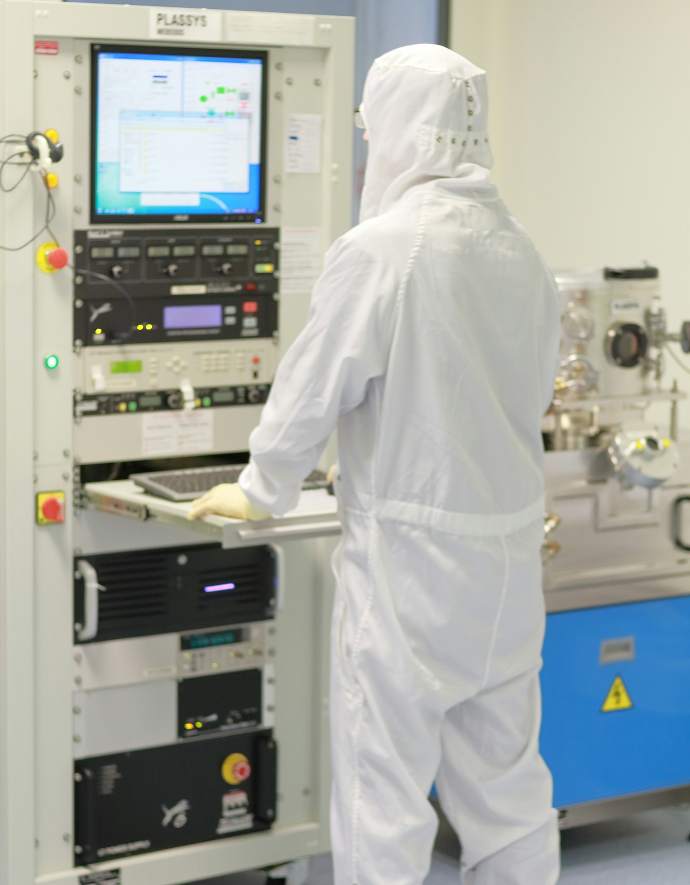 02
02Through precise control of temperature, pressure, flow, and vaporization systems, we are developing a next-generation furnace that deposits atomic-layer thin films (ALD).
By securing the uniformity and stability of High-k dielectric processes, it addresses advanced semiconductor processes.
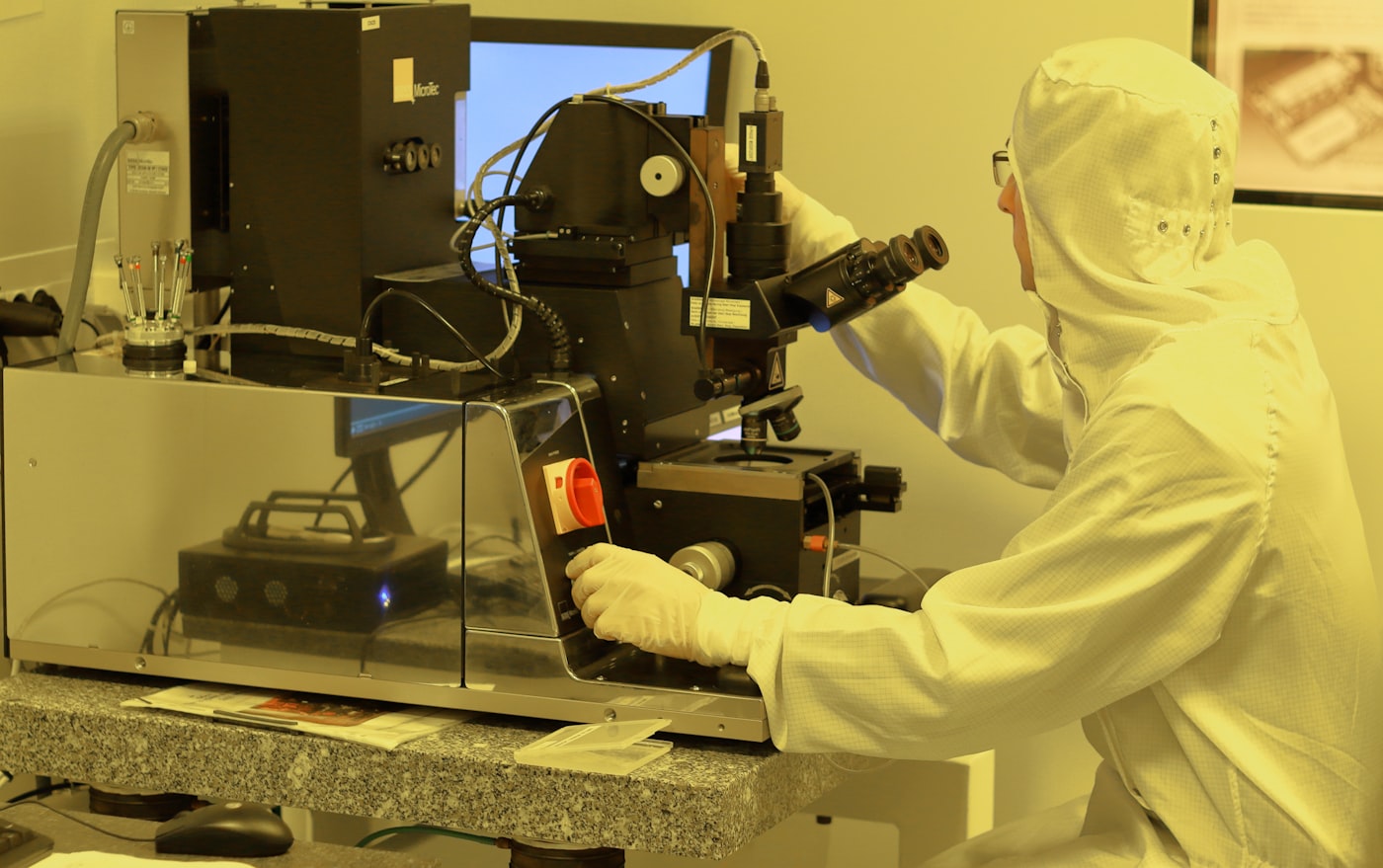
We research process equipment that removes fine bubbles and cures the surface of substrates coated with an interlayer insulating material (CCL Film).
By minimizing VOID and increasing adhesion strength, it improves the quality and reliability of display processes.
 03
03 04
04We are conducting research to improve the efficiency and durability of AEM (Anion Exchange Membrane) water electrolysis systems,
and are securing scale-up technology from small- and mid-scale to MW-scale, large-capacity systems.
Through green hydrogen production linked to renewable energy, we are preparing for carbon neutrality.
Through relentless technological innovation,
we set the standard for future processes.